PCB design service and turnkey electronic engineering solutions.                                                                                            Phone: 407-340-2668

Apycom Java Applets

PCB Design Service based in USA
  Contact Info:
 
Saturn PCB Design, Inc.

Phone: 407-340-2668
Fax: 386-789-2765
email:
sales@saturnpcb.com

 
  Free PCB Toolkit:


Download the Saturn PCB Toolkit.


Top 5 myths about using a PCB design service.

Myth 1:
Using an outside PCB design firm is way too expensive.

Truth:
Our average turn time is far better than most companies are used to which in turn saves them quite a bit of money.

Myth 2:
Our internal processes and procedures are too complicated to have an outsider work with us.

Truth:
Our designers have worked at some of the world’s largest companies and we are all very familiar with complex internal procedures and processes.

Myth 3:
Our products are too advanced for an outsider to understand.

Truth:
We have worked on many highly advanced products and are specialists in HDI, RF and EMI sensitive designs.

Myth 4:
We use a certain PCB design program here; I doubt you have it there.

Truth:
There is no PCB design software package that we either don’t already own or can’t get in order to complete your project.

Myth 5:
We need to start this project right away and don’t have time to put an extensive package together for a design firm to quote.

Truth:
Usually, a PCB design project can be quoted with just a schematic and simple statement of work. If needed, we will come to you when we kick the project off. For a complete engineering project, we can produce a ROM from a statement of work.


  PCB Design Services

Saturn PCB has the tools and knowledge to design your PCB no matter how large or small.
We use the industries top tier design tools and are driven to be the best.
Just fill out the
on-line quote form to get started.

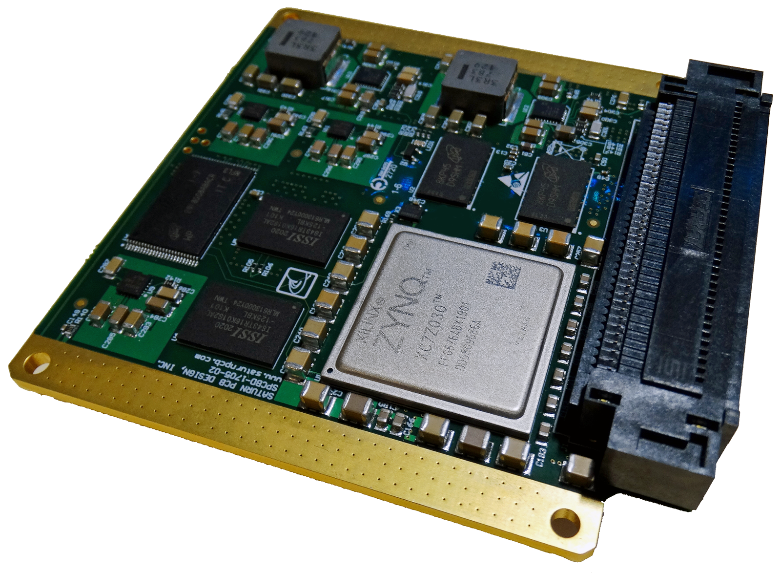
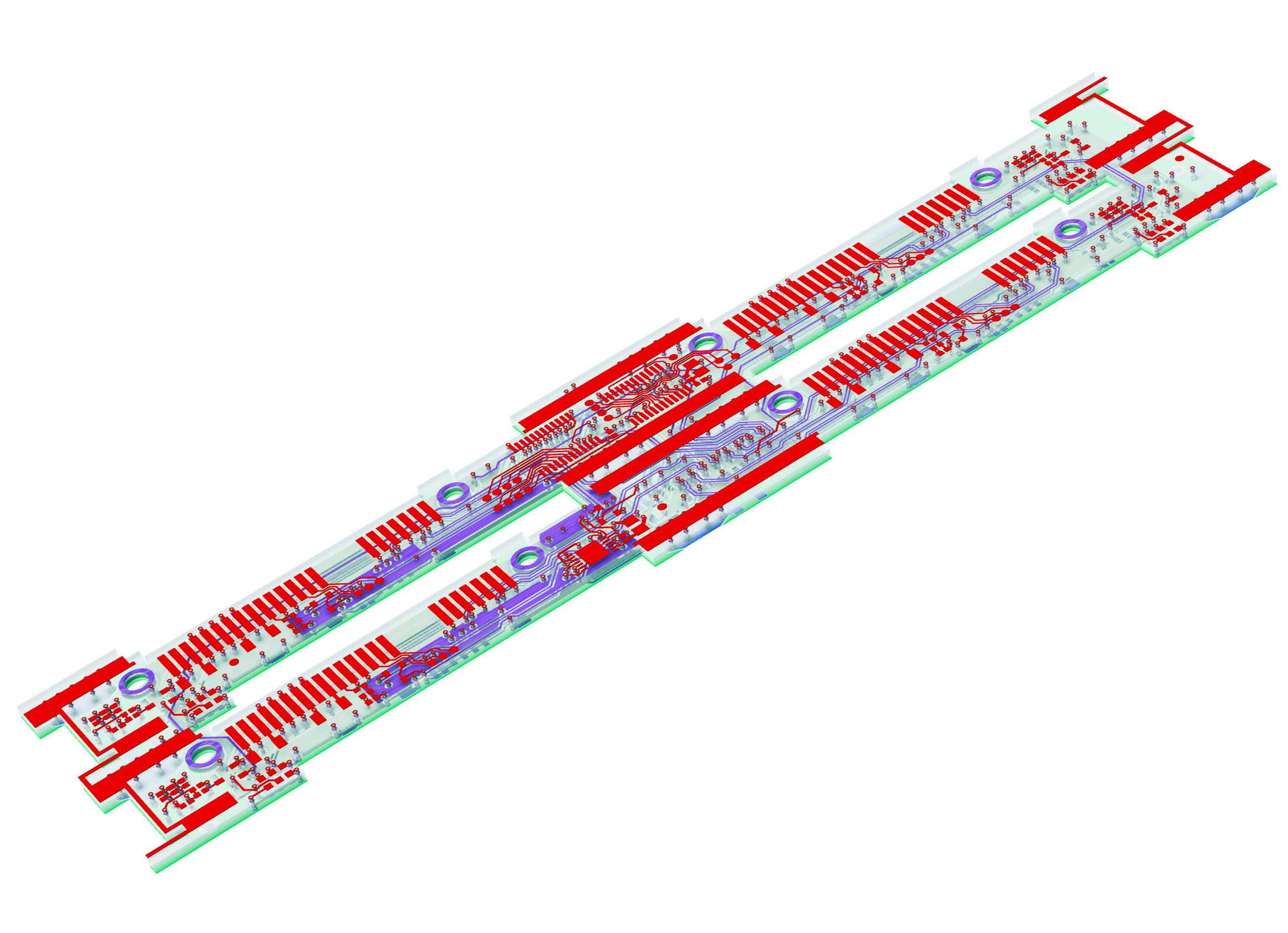
  • HDI Designs with micro vias and advanced materials - Via-in-Pad, laser micro vias, ALIVH technology.
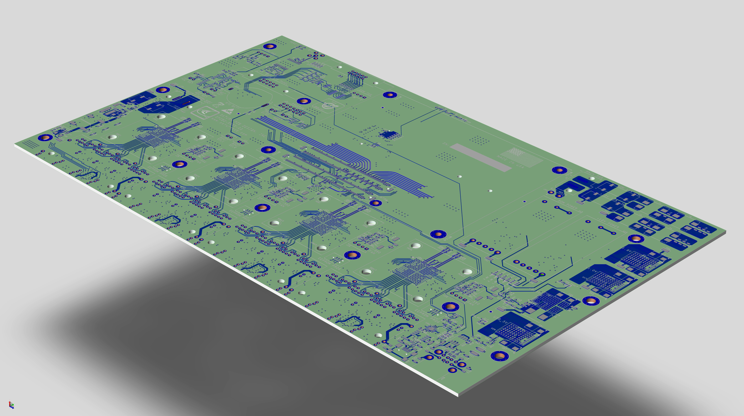
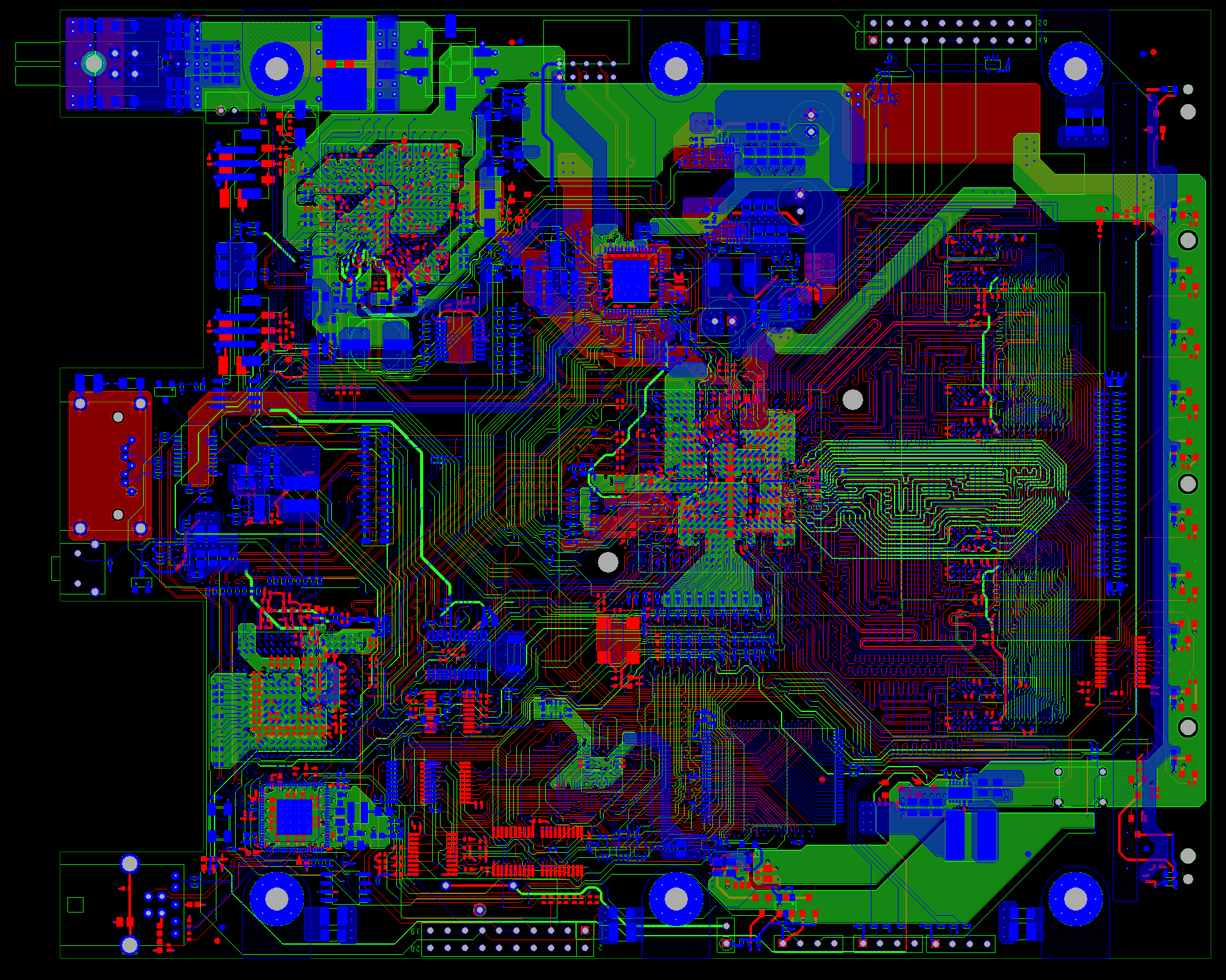
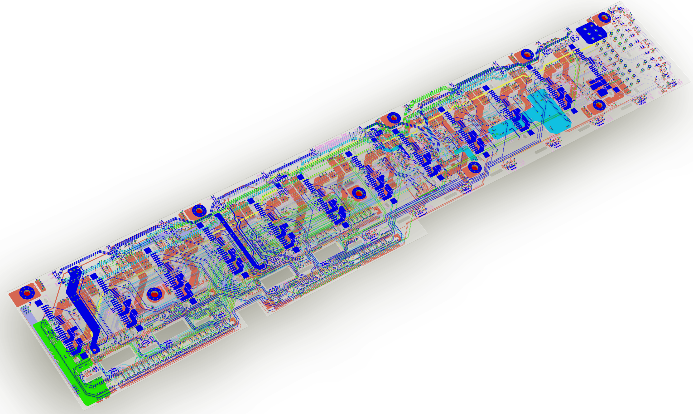
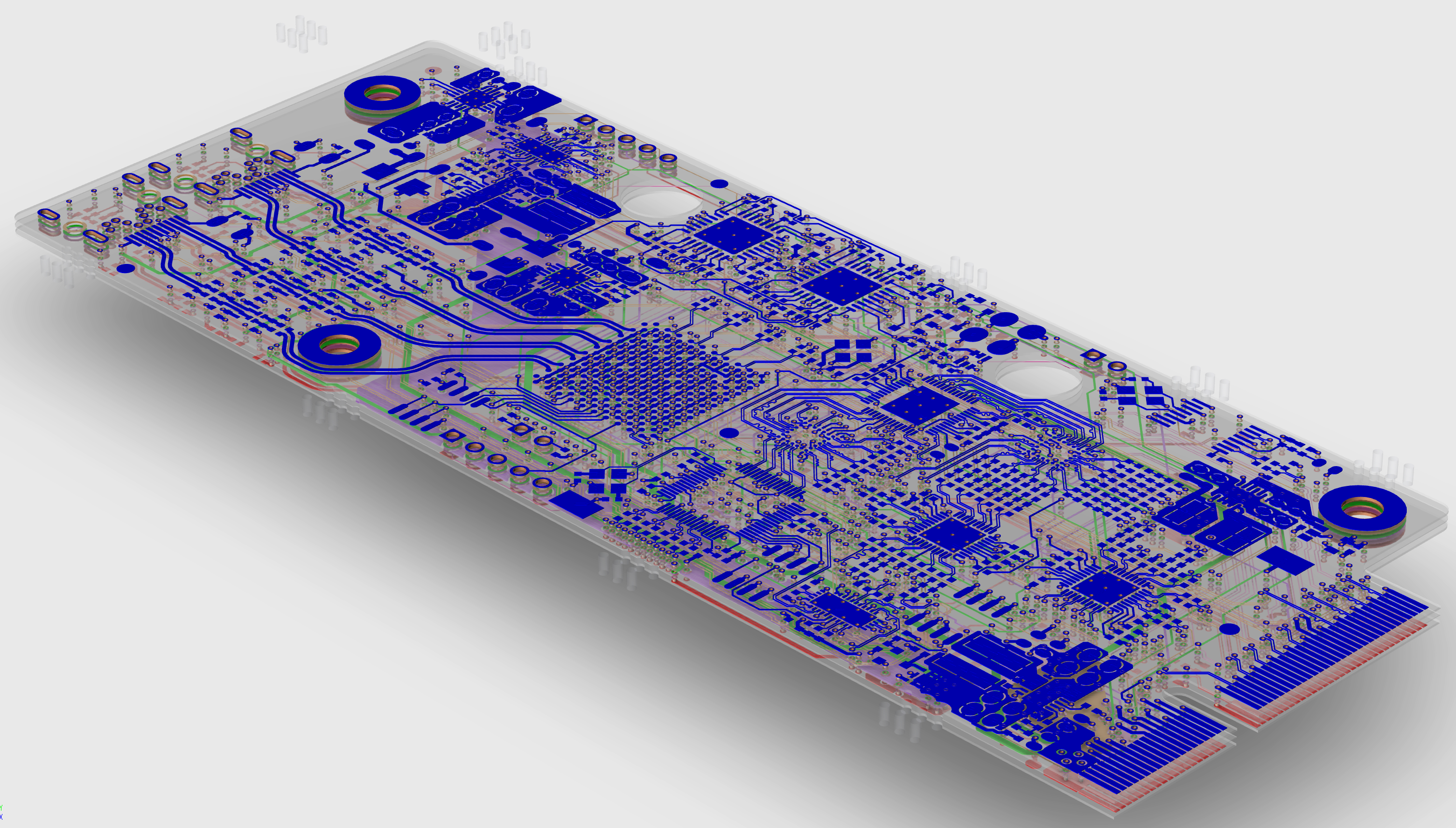
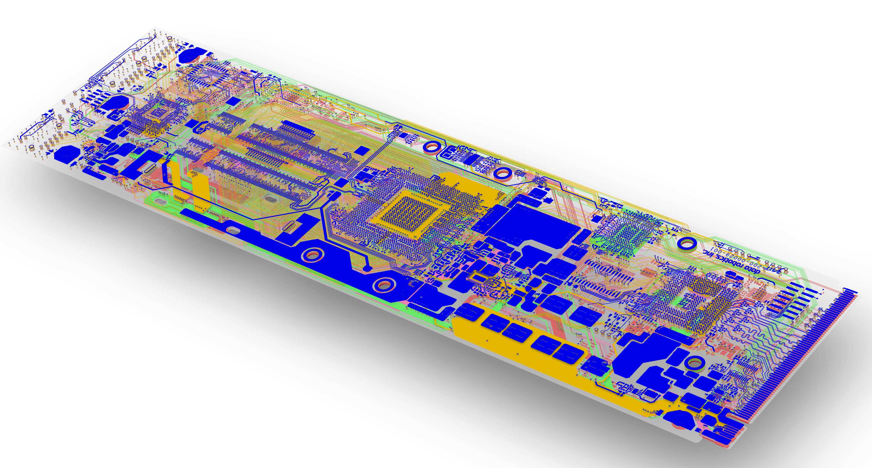
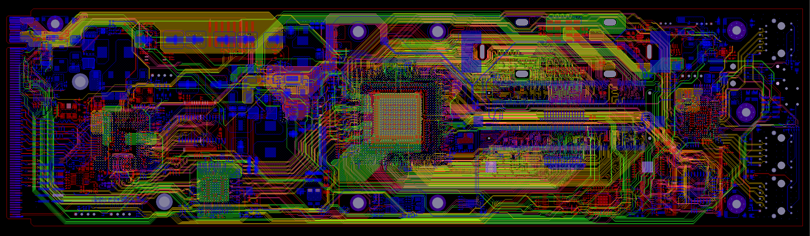
  • High speed, multi layer digital PCB designs - Bus routing, differential pairs, matched lengths.
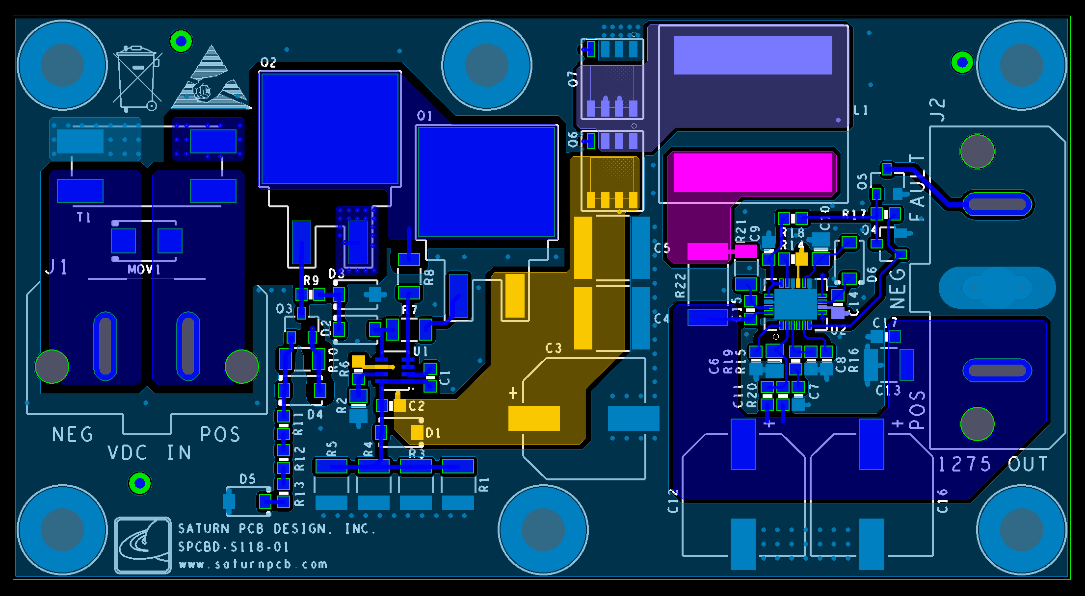
  • PCB Designs for space, military, medical and commercial applications
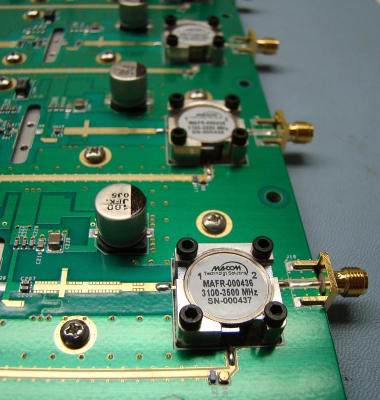
  • Extensive RF and analog design experience (printed antennas, guard rings , RF shields...)
  • Signal integrity issues to meet your digital design needs (tuned traces, diff pairs...)
  • PCB Layer management for signal integrity and impedance control
  • DDR, DDR2, DDR3, SAS and differential pair routing expertise
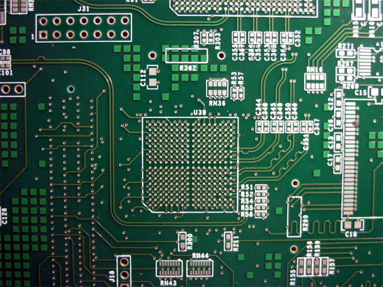
  • High density SMT designs (BGA, uBGA, PCI, PCIE, CPCI...)
  • Flex PCB designs of all types
  • Low level analog PCB designs for metering
  • Ultra low EMI designs for MRI applications
  • Complete assembly drawings
  • In-Circuit Test data generation (ICT)
  • Drill, panel and cutout drawings designed
  • Professional fabrication documents created
  • Autorouting for dense PCB designs


500 MHz PulseBlasterESR, Dual Core

PCIe Card with SATA routing.

40GHz COB Amplifier board

40GHz. Wire Bonded Chip-on-Board Amplifier PCB.

Micro BGA HSD PCB Design

HSD PCB Design

  Signal Integrity Simulation

No one outperforms Saturn PCB Design, Inc. when it comes to understanding SI issues, analysis and resolution
in the PCB layout arena. We know how to manage your layer stack up and trace widths to meet the desired
impedance and we know what to look for in SI management to make your design work as it should.


©2010 Saturn PCB Design, Inc. All rights reserved.

2737 Bishop Lane Deltona, Florida 32725 :: (407) 340-2668
All trademarks and registered trademarks are the property of their respective owners.
Send your comments about this site to webmaster@saturnpcb.com
View Saturn PCB Design's Privacy Policy