
NOTE:
In order to understand the PCB Toolkit version differences, I have added this brief description of the version series. If you are not yet familiar with the IPC-2152,then please be aware that there are two separate charts for finding conductor (or via) current vs. temperature rise.
PCB Toolkit Version 8 series:
No longer uses multipliers for cross sectional area as related to the IPC-2152.
PCB Toolkit Version 7 series:
Functionally the same as the series 6 as related to the IPC-2152.
PCB Toolkit Version 6 series:
Functionally the same as the series 5 as related to the IPC-2152.
PCB Toolkit Version 5 series:
This version uses the IPC-2152 “conservative” chart for finding conductor current vs. temperature rise and also adds the ability to include other PCB parameters that can affect temperature rise (like PCB thickness and plane usage). We have also been working on developing our own formulas for current to get as close as possible to the measured data charts of the IPC-2152. We feel that all values in the version 5 series are within +/-10 of measured values plotted on the charts.
PCB Toolkit Version 4 series:
This version uses the IPC-2152 “conservative” chart for finding conductor current vs. temperature rise. The conservative chart in the IPC-2152 is really just the internal chart from the IPC-2221 so that was the formula used. Version 4 series is accurate to the IPC-2152 but may be too conservative in many cases.
PCB Toolkit Version 3 series:
This version uses the IPC-2221 formula for finding conductor current vs. temperature rise. The IPC-2221 has been superseded by the IPC-2152 for finding conductor current vs. temperature rise and is now obsolete.
Does not apply to V8.0 or higher:
Please note that when using the IPC-2152 with modifiers option, the amperage value has a slight drop at 10,20,30,40,50,60,70,80,90,100,200,300,400,500,600 & 700sqmils. This is due to a multiplier used for each cross sectional area range. All values are within +/-10% of the chart values however. If you do not need to minimize conductor width on your PCB, you can use the IPC-2152 without modifiers option where there is no multiplier effect.
Saturn PCB Toolkit Help
Version 8.20
Bandwidth & Max Conductor Length
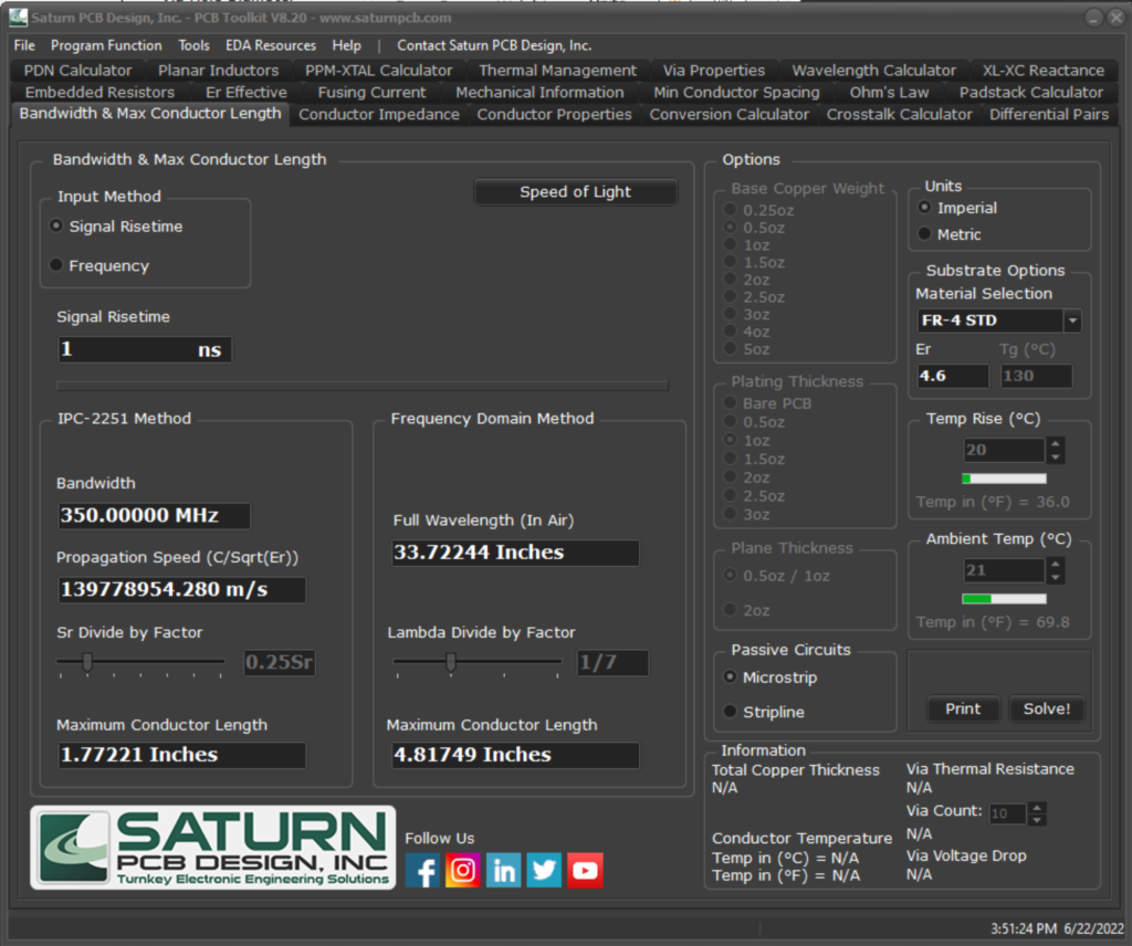
This tool calculates the maximum length of a conductor before it should be considered a transmission line subject to signal integrity or impedance matching concerns.
Input Method:
Select between entering the signal risetime or the frequency.
IPC-2251 Method:
This calculator uses the signal risetime along with the Er of the substrate to determine maximum length.
Sr Divide by Factor:
Use the slider to change the Sr (rise distance) divide factor. A typical value of 0.25Sr is set by default.
Maximum Conductor Length:
This is the maximum length the conductor before it should be considered a transmission line. If your conductor is shorter than this value, it generally does not need to be impedance controlled.
Passive Circuits:
Select between microstrip or stripline. This option is only available when signal risetime is the selected input method and only affects the IPC-2251 calculator.
Frequency Domain Method:
This calculator uses the frequency, either entered or calculated from risetime, to find the full wavelength in air and divide from that. It does not use Er or circuit type. A typical value of 1/7 Lambda has been set by default.
Conductor Impedance
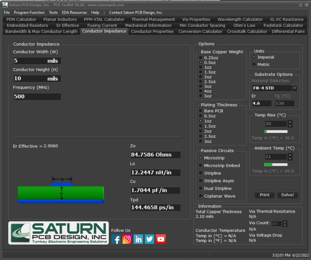
This tool calculates the impedance of a conductor based on various inputs and circuit type.
Conductor Width:
This is the width of the conductor.
Conductor Height:
This is the height of the conductor (distance) above the reference plane.
Frequency:
When Microstrip is selected, the user can enter frequency. This causes a slight change in Er effective which in turn causes a slight change in impedance.
Zo:
This is the impedance of the conductor based on the given inputs.
Lo:
This is the inductance of the conductor based on the given inputs.
Co:
This is the capacitance of the conductor based on the given inputs.
Tpd:
This is the propagation delay a signal will incur through the conductor.
Conductor Properties
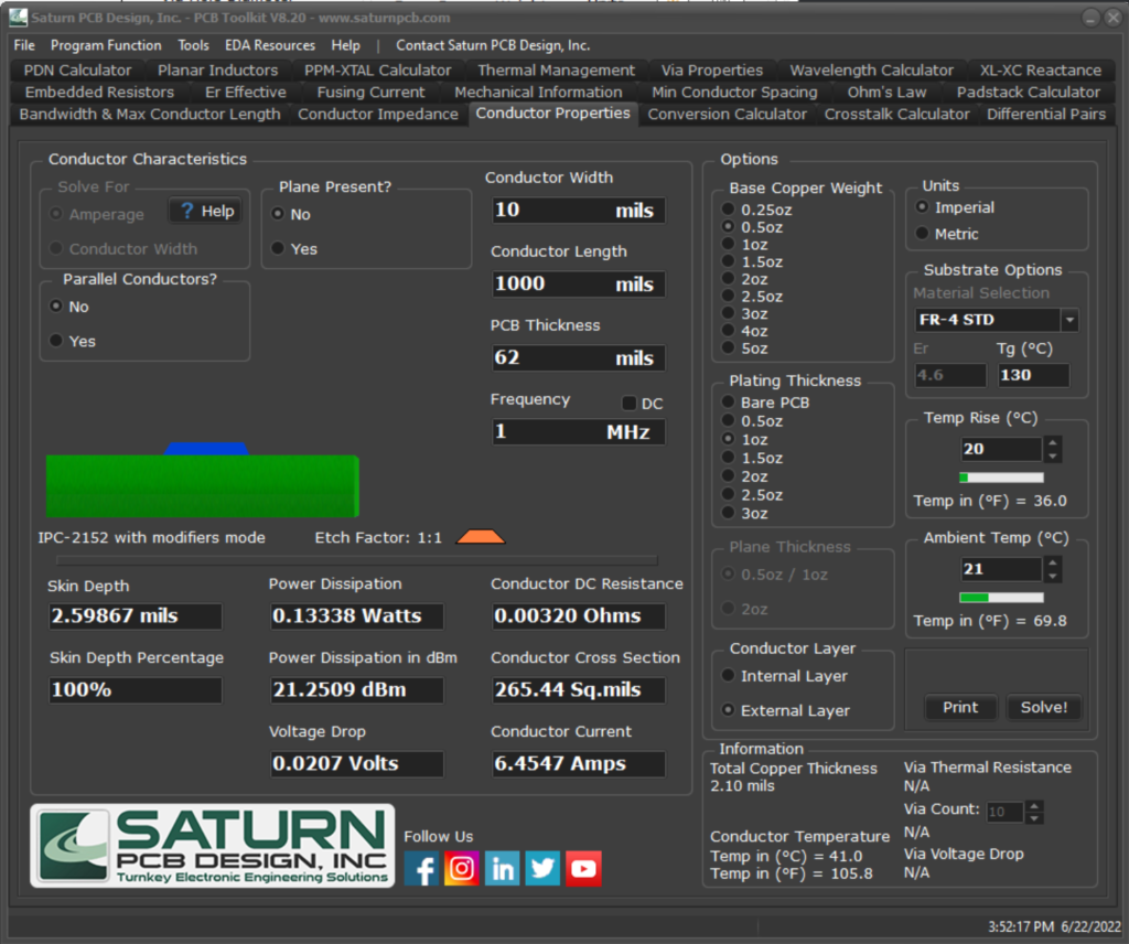
This tool calculates current vs temperature rise in a conductor along with various other items.
Solve For:
Amperage: Sets solving for amperage as the priority where conductor width is the input.
Conductor Width: Sets solving for conductor width as the priority where amperage is the input.
This selection is only enabled for the IPC-2152 Without Modifiers and the IPC-2221 options. See Program Options to change settings.
Conductor Layer:
Select between an internal or external conductor.
Plane Present:
Select if a plane is present in your design. A copper plane will help dissipate heat away from the conductor.
Plane Thickness:
Select between one of the two preset thicknesses for the plane. This tool cannot determine with accuracy a plane greater than 2oz. thick.
Distance to Plane:
If Plane Present is set to “Yes”, this option becomes available. Enter the distance between the conductor and plane.
Parallel Conductors:
Select when trying to determine the effect of parallel conductors on current vs temperature rise.
Parallel Conductor Count:
If Parallel Conductors is set to “Yes”, this option becomes available. Enter the number of parallel conductors to be factored in.
Conductor Width:
Enter the width of the conductor.
Conductor Length:
Enter the length of the conductor.
PCB Thickness:
Enter the overall thickness of the PCB. The thickness of the PCB plays a role in current vs temperature rise as the substrate acts as a heat sink.
Frequency:
Enter the frequency, if any, of a signal through the conductor. The field is only necessary for skin depth and has no influence on current vs temperature rise.
Load Current:
Enter the load current flowing through the conductor. NOTE: This is separate from “Conductor Current” which is a calculated value based on temperature rise. Entering a load current allows the tool to find the voltage drop and temperature of a conductor based on the entered value.
Conductor DC Resistance:
This is the DC resistance of the conductor based on its width and length.
Total Cross Section:
This is the area of a cross section of the conductor. This can change with etch factor as is used to determine conductor current.
Temp Rise:
Set the maximum temperature rise allowed in the conductor by way of current flowing through it.
Ambient Temp:
Set the ambient temperature of the PCB, this will be added to temp rise to determine the total temperature of the conductor once current flows through it.
Conductor Current:
This is the calculated amount of current that will cause the temperature of the conductor to rise, above ambient, to the set temperature. This IS NOT the maximum current the conductor can handle before burning up. In the above example, 4.381A will cause a 50mil wide conductor to rise 20C above ambient.
If the ambient temperature + temp rise selected is greater than the selected material’s Tg value, a warning will appear stating that the maximum material temperature has been exceeded.
Distance to Plane:
If Plane Present is set to “Yes”, this option becomes available. Enter the distance between the conductor and plane.
Power Dissipation:
This is the power dissipated by the conductor based on DC resistance and voltage drop.
Power Dissipation in dBm:
This is the power dissipated by the conductor based on DC resistance and voltage drop expressed in decibels.
Voltage Drop:
This is the voltage drop across the conductor based on the derived values of current and DC resistance.
Loaded Voltage Drop:
This is the loaded voltage drop across the conductor based on the entered values of load current and the derived value of DC resistance.
Skin Depth:
Skin depth is a measure of how far electrical conduction takes place in a conductor based on frequency.
https://www.microwaves101.com/encyclopedias/skin-depth
Skin Depth Percentage:
This is the percentage of the skin depth in the conductor.
Conversation Conductor
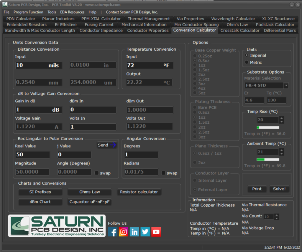
This tool performs an array of mathematical conversions and has links to online charts for reference.
Distance Conversion:
Convert primarily between mils and millimeters. Other converted values are also shown in the disabled edit boxes.
Temperature Conversion:
Convert between Celsius and Fahrenheit.
dB to Voltage Gain Conversion:
Convert between gain in decibels and voltage gain.
dBm Out:
Adds the gain and dBm in values for a theoretical lossless dBm out value.
Volts Out:
This is the dBm out value converted to voltage.
Rectangular to Polar Conversion:
Convert between rectangular values and polar values.
Angular Conversion:
Convert between degrees and radians.
Send:
Sends the angular degrees, converted from the R+jX input, to the Angular Conversion calculator to be converted to radians.
Charts and Conversions:
Links to various online resources. Your default browser will be spawned.
Differential Pairs
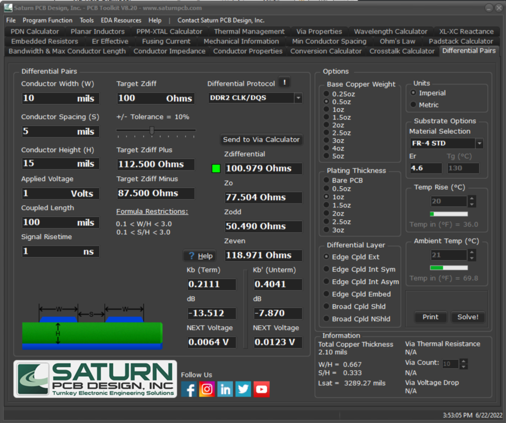
This tool calculates the differential impedance of a coupled pair as well as the NEXT (Near-End Crosstalk). Use this tool to whether the coupled pair is carrying a true differential signal or not, the math is the same for crosstalk.
W/H:
Ratio of conductor width vs. conductor height.
S/H:
Ratio of conductor spacing vs. conductor height.
Note:
Warning! simply means the data is out of range for the formula and is a warning to avoid microstrip line models.
Target ZDiff:
Enter the target differential impedance. The indicator to the right of the ZDifferential edit box will show green when the calculator output is within tolerance and red when out of tolerance.
+/-Tolerance:
This is the Target ZDiff + and – a value given by the slider bar. 10% is a typical acceptable tolerance for a differential pair and is set as the default value.
Target ZDiff Plus:
This is the Target ZDiff plus selected percentage.
Target ZDiff Minus:
This is the Target ZDiff minus selected percentage.
Zo:
Impedance of one single conductor in the differential pair.
Zdifferential:
Differential impedance of the pair. A common impedance for a balanced line is 100ohms, but can be any value, and can be achieved by changing any of the input parameters.
Zodd:
This is the odd-mode impedance of the differential pair.
Zeven:
This is the even-mode impedance of the differential pair.
NOTE: The formulas used in the program are valid for 0.1<W/H<3.0 and 0.1<S/H<3.0.
Differential Protocol:
Select the desired protocol from the dropdown list, this list will autofill the Target ZDiff edit box.
Crosstalk Area of the Differential Calculator:
Use this tool to calculate NEXT (Near-End Crosstalk) weather the signal is a true differential or not, the calculation is the same.
Applied Voltage:
Enter the applied voltage level of the signal.
Coupled Length:
Enter the distance that the two conductors are considered to be coupled.
Signal Risetime:
Enter the risetime of the signal in nanoseconds.
Kb:
This is the coupling coefficient of a terminated pair.
Kb’:
This is the coupling coefficient of an unterminated pair.
dB:
This is the coupling coefficient in terms of decibels.
NEXT Voltage:
This is the near-end coupled voltage based on signal risetime, applied voltage and coupled length.
Lsat:
This is the “saturated length” based on the dielectric constant of the material and conductor geometry.
The NEXT voltage will increase with coupled length up to the point of Lsat where at that point the coupled length no longer plays a role in near-end crosstalk.
Embedded Resistors
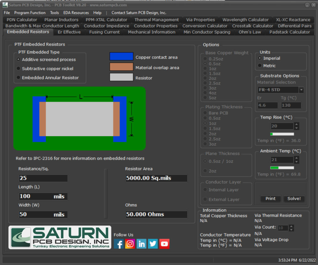
This tool helps to determine the size of an embedded resistor based on geometry and material resistance.
Resistance/Sq.:
Enter the resistive value of the material in per square inches / millimeters.
Length:
Enter the length of the embedded material to be placed in the PCB.
Width:
Enter the width of the embedded material to be placed in the PCB.
Ohms:
This is the calculated resistance of the embedded device.
Er Effective
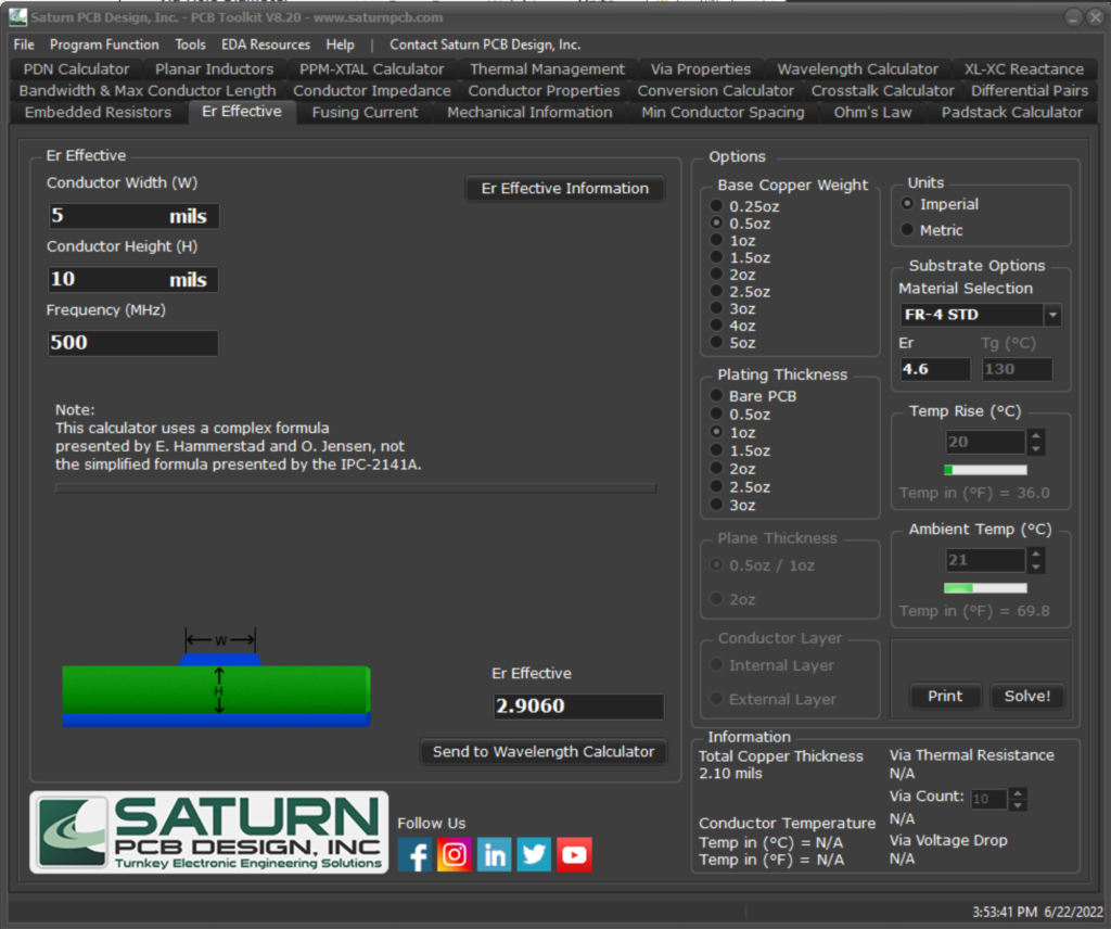
Er Effective takes microstrip geometry into account and is used instead of Er in calculations.
https://www.microwaves101.com/encyclopedias/keffective
Conductor Width:
This is the width of the conductor.
Conductor Height:
This is the height of the conductor (distance) above the reference plane.
Frequency:
Enter the signal frequency. This causes a slight change in Er effective.
Fusing Current
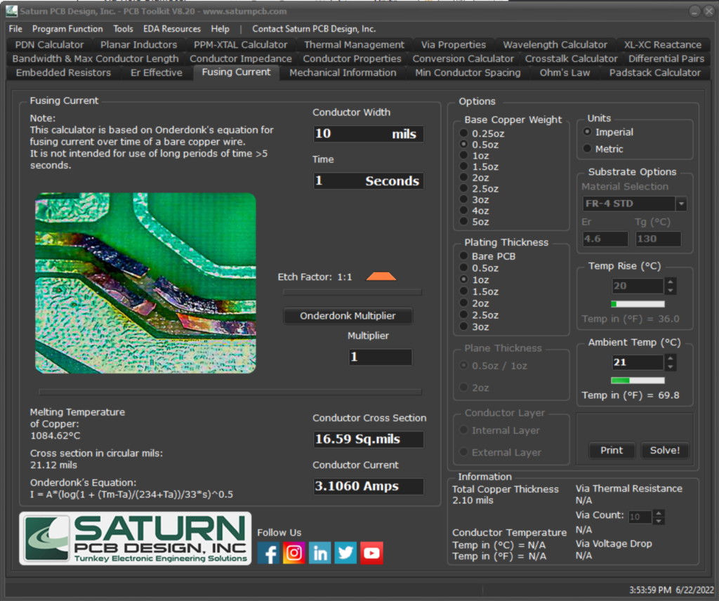
This tool calculates the fusing current of a copper conductor based on its width and amount of time the current is flowing through it.
Conductor Width:
This is the width of the conductor
Time:
This is the time the conductor, with the given width, will last with the calculated amperage flowing through it.
The formula is untested and is primarily used for higher current applications with short fuse times.
Onderdonk Multiplier:
Some work has been done to improve the accuracy of this formula and a multiplier system has been implemented. Enter that multiplier here.
https://www.pcdandf.com/pcdesign/index.php/magazine/10293-pcb-design-1509
Conductor Cross Section:
This is the area of a cross section of the conductor. This can change with etch factor as is used to determine conductor current.
Conductor Current:
This is the approximated current that will cause a failure in the conductor due to heating.
Note:
Fuse current value is determined by Onderdonk’s equation. This was originally developed for bare copper in air and has been adapted to PCB’s. This is only an estimate as there is no empirical data to back up this equation as it relates to PCB’s.
Mechanical Information
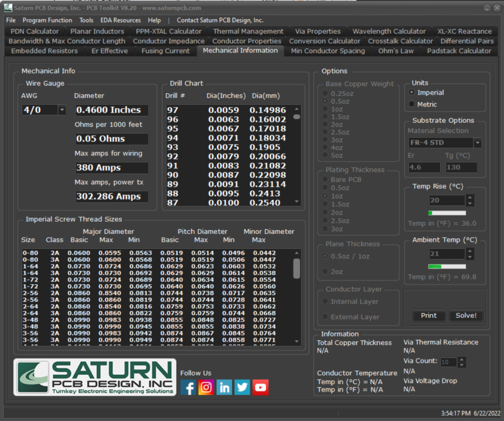
Wire Gauge:
Select the wire gauge from a dropdown list to see diameter, ohms per unit length and amperage.
Drill Chart:
Typical, but not all inclusive, of a drill chart used in PCB manufacturing.
Screw Thread Sizes:
Basic chart of imperial and metric screws and their associated diameters.
Minimum Conductor Spacing
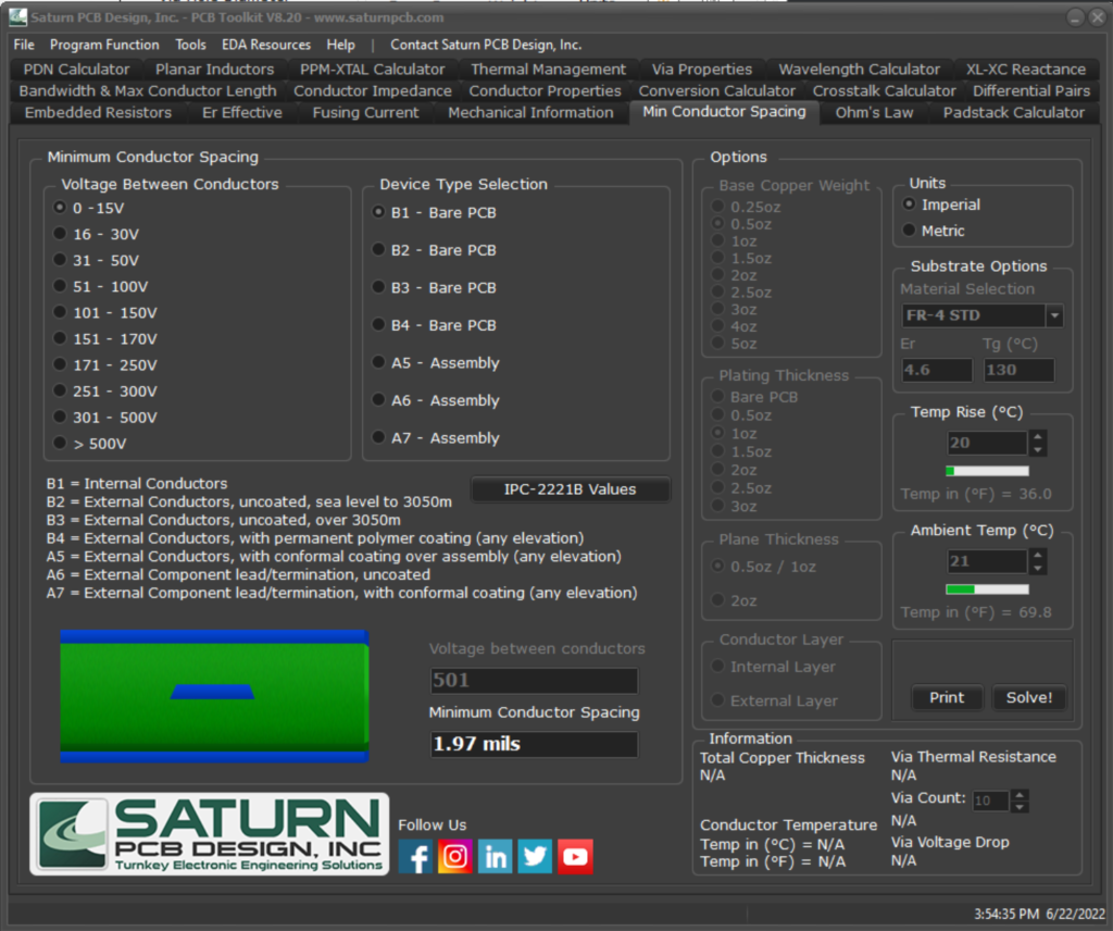
Based off the IPC-2221B specification, this tool displays a minimum conductor spacing based on the voltage and type of circuit selected.
Voltage Between Conductors:
Select from a list of pre-determined voltage ranges.
Voltage Between Conductors (edit box):
If 500>is selected from the list, this edit box will become available. Here the user enters the voltage level to be calculated.
Device Type Selection:
Select from a list of pre-determined device types such as bare boards or assemblies.
Minimum Conductor Spacing:
This is the minimum spacing value between PCB conductors needed in order to meet the IPC-2221B specification.
https://www.ipc.org/ipc-standards
Ohms Law
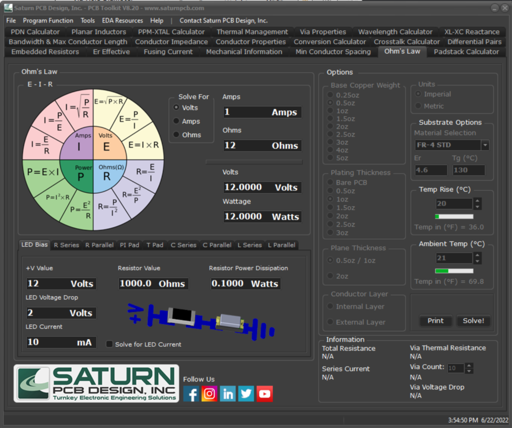
This tool calculates basic ohms law as well as other RLC configurations.
LED Bias:
+V Value:
Enter the supply voltage the LED is connected to.
LED Voltage Drop:
Enter the voltage drop of the LED, see part datasheet.
LED Current:
Enter the desired LED current.
Resistor Value:
This is the calculated resistor value needed to run the LED at the given current.
R Series / R Parallel:
Select from between 2 and 4 series or parallel resistors to find the total resistance.
Voltage:
Enter a voltage to be seen across the series or parallel resistors. This will determine the individual resistor amperage and wattage based on the resistor values inputted.
PI Pad:
A PI PAD is used in RF circuits as an attenuator. This tool calculates the resistor values needed to achieve the given attenuation.
T Pad:
A T PAD is used in RF circuits as an attenuator. This tool calculates the resistor values needed to achieve the given attenuation.
Attenuation:
Enter the amount, in decibels, the PI or T PAD needs to attenuate.
Zin:
Enter the impedance seen at the PI or T PAD’s input.
Zout:
Enter the impedance seen at the PI or T PAD’s output.
C Series / C Parallel:
Select from between 2 and 4 series or parallel capacitors to find the total capacitance.
L Series / L Parallel:
Select from between 2 and 4 series or parallel inductors to find the total inductance.
Padstack Calculator
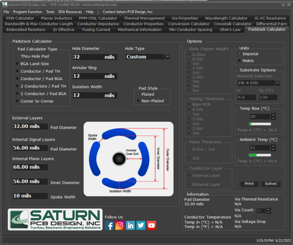
Thru-Hole Pad:
Hole Type:
Select from a list of pre-determined hole diameter values or select “custom” to enter your own values.
Hole Diameter:
Enter the finished hole diameter of the pad.
Pad Style:
Select between a plated or non-plated hole.
Annular Ring:
Enter the minimum annular ring allowed for this padstack. Annular ring is the distance from the outer edge of the copper to the outer edge of the finished hole.
Isolation Width:
Enter the desired isolation width of the thermal opening (air gap).
External Layers:
This is the calculated pad diameter for the outer layers based on the given inputs.
Internal Signal Layers:
This is the calculated pad diameter for the inner signal layers based on the given inputs. Some designs require a larger pad diameter for inner signal layers, if your design does not require this the outer layer diameter can be used.
Internal Plane Layers:
This is the calculated pad diameter for the inner plane layers based on the given inputs. Some designs require a larger pad diameter for plane layers, if your design does not require this either the inner signal layer diameter or the outer layer diameter can be used.
Inner Diameter:
If your padstack is using a thermal relief, this value would be used as the inner layer diameter.
Spoke Width:
This is a suggested width of the thermal spoke. Your design may require a different value as this is just a suggestion.
BGA Land Size:
Nominal Ball Diameter:
Select from a list of BGA ball diameters. This value should be found in the BGA’s datasheet.
Nominal Land Diameter:
This value is the average PCB land diameter that could be used with the selected ball diameter.
Land Variation:
These values are the upper and lower limits of the land diameter that should be used in the design. Note that the IPC-7351A specification uses the larger land variation diameter for the proper BGA land size.
Conductor / Pad TH:
Distance Between Pads:
Enter the distance between the thru-hole pad centers that the conductor must fit through.
Conductor Width:
Enter the width of the conductor that must travel between the two pads.
Spacing Constraint:
Enter the spacing constraint set up in the design for the appropriate entities. Typically, this is called out as Pad to Conductor spacing.
Hole Diameter:
Enter the finished hole diameter of the pad.
Minimum Annular Ring:
Enter the minimum annular ring allowed by the design constraints for a thru-hole padstack.
Maximum Pad Diameter:
This is the maximum pad diameter that should be used to fit a conductor, of desired width, through them.
Calculated Annular Ring:
This is the calculated value of annular ring of the padstack per the given inputs. If the calculated annular ring is smaller than the minimum annular ring allowed, a warning will appear.
Conductor / Pad BGA:
Distance Between Pads:
Enter the distance between the BGA pad centers that the conductor must fit through.
Land Diameter:
Enter the diameter of the BGA lands in the design.
Spacing Constraint:
Enter the spacing constraint set up in the design for the appropriate entities. Typically, this is called out as SMD Pad to Conductor spacing.
Maximum Conductor Width:
This is the widest conductor that will fit between the given BGA lands.
2 Conductors / Pad TH:
Distance Between Pads:
Enter the distance between the thru-hole pad centers that the two conductors must fit through.
Conductor Width:
Enter the width of the two conductors that must travel between the two pads. This is mostly used for differential pairs.
Spacing Constraint:
Enter the spacing constraint set up in the design for the appropriate entities. Typically, this is called out as Pad to Conductor spacing.
Hole Diameter:
Enter the finished hole diameter of the pad.
Minimum Annular Ring:
Enter the minimum annular ring allowed by the design constraints for a thru-hole padstack.
Maximum Pad Diameter:
This is the maximum pad diameter that should be used to fit a pair of conductors, of desired width, through them.
Calculated Annular Ring:
This is the calculated value of annular ring of the padstack per the given inputs. If the calculated annular ring is smaller than the minimum annular ring allowed, a warning will appear.
2 Conductors / Pad BGA:
Distance Between Pads:
Enter the distance between the two BGA pad centers that the conductors must fit through.
Land Diameter:
Enter the diameter of the BGA lands in the design.
Spacing Constraint:
Enter the spacing constraint set up in the design for the appropriate entities. Typically, this is called out as SMD Pad to Conductor spacing.
Maximum Conductor Width:
This is the maximum width of the two conductors that will fit between the given BGA lands.
Corner to Corner:
Length of side a:
Enter the length of side “a” of a square or rectangular pin.
Length of side b:
Enter the length of side “b” of a square or rectangular pin.
Distance Between Corners:
This is the hypotenuse value (distance between corners) for the give pin inputs.
Suggested Min Drill:
This is a suggested drill diameter minimum that should be used with the given pin.
Suggested Max Drill:
This is a suggested drill diameter maximum that should be used with the given pin.
PDN Calculator
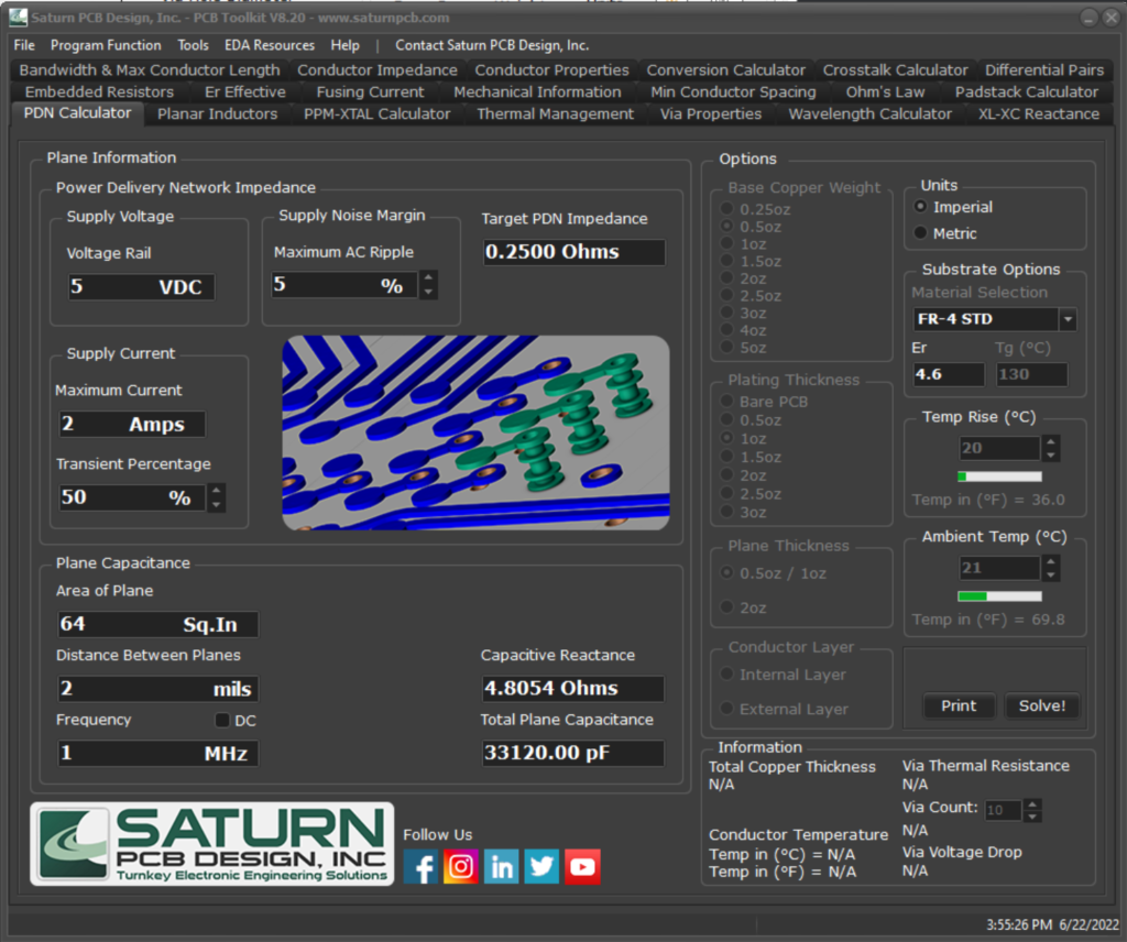
Power Delivery Network Impedance:
Voltage Rail:
This is the dc potential of the power rail.
Maximum Current:
This is the maximum current seen on the given power rail.
Transient Percentage:
This is the percentage of the rail current that is transient, or being switched, that the plane will see.
Maximum AC Ripple:
This is the maximum AC ripple allowed on the given power rail.
Target PDN Impedance:
This is calculated impedance of the PDN per the given inputs.
Plane Capacitance:
Area of Plane:
Enter the area of the copper plane in square inches or mm.
Distance Between Planes:
Enter the distance, or separation, between the two planes.
Frequency:
Enter the frequency, if any, seen on the planes.
Capacitive Reactance:
This is calculated Xc of the two parallel planes.
Total Plane Capacitance:
This is calculated capacitance of the parallel planes.
Planar Inductors
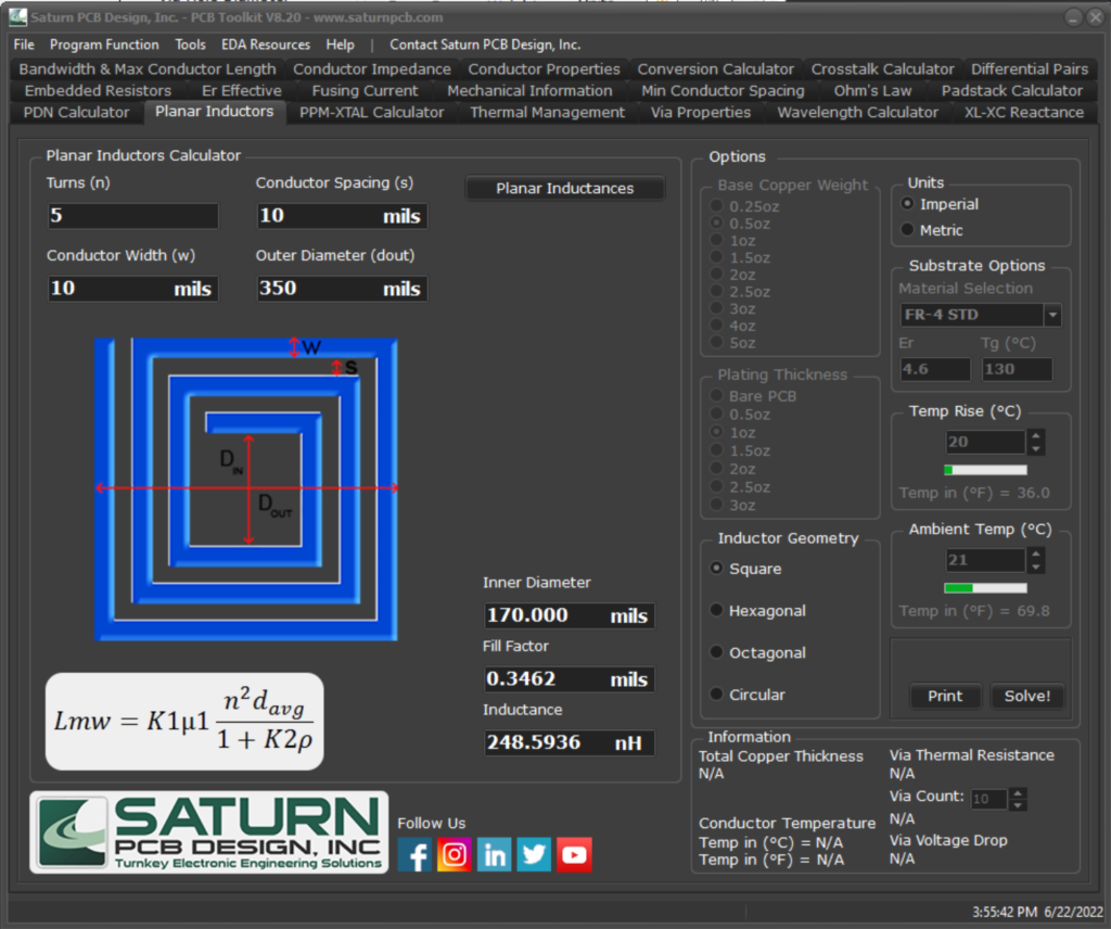
Use this tool to calculate the inductive value of square, hexagonal octagonal and circular planar PCB inductors.
Turns:
This is the total number of turns on the printed planar inductor.
Conductor Width:
This is the line width of the conductor being used in the planar structure.
Conductor Spacing:
This is the spacing between conductors in the planar structure.
Outer Radius:
This is the radius of the planar structure measured from the center of the structure to the outer edge of the outermost winding.
Inner Diameter:
This is the calculated inner diameter of the planar PCB inductor.
Fill Factor:
This is the calculated “average” diameter of the planar inductor.
p = (dout-din)/(dout+din).
Inductance:
This is the calculated inductance of the planar inductor.
PPM-XTAL Calculator
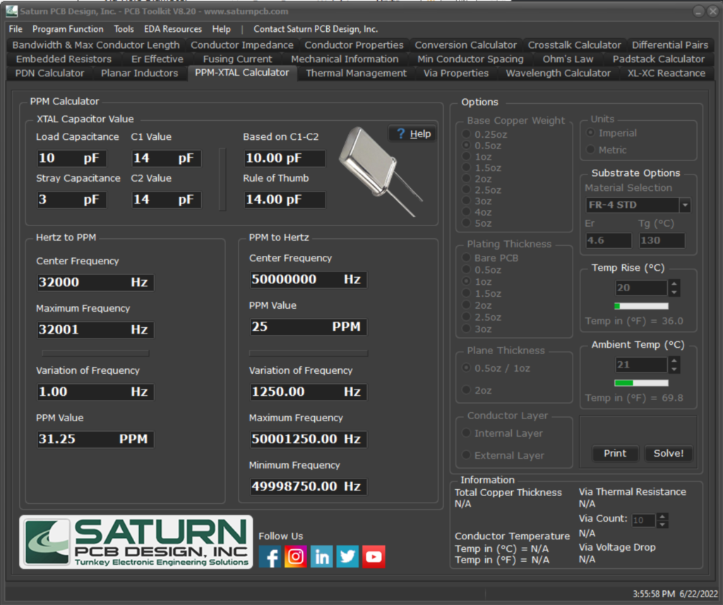
XTAL Capacitor Value:
Load Capacitance:
Enter the load capacitance of the XTAL, this is usually found in the part datasheet and is called out in picofarads.
Stray Capacitance:
Enter the estimated stray capacitance seen in the pads / conductors of the PCB routing to / from the XTAL.
C1 – C2 Value:
Enter a value for C1 and C2 if you have already selected them.
Based on C1–C2:
This is a calculated value based on load and stray capacitance as well as the entered C1-C2 values. This should match the load capacitance called out in the datasheet of the part, if it does not then C1 and C2 should be adjusted until it does.
Rule of Thumb:
If you have not yet selected a value for C1 and C2, this “rule of thumb” can be used as a starting point. It is based solely off the load and stray capacitance inputs.
PPM to Hertz:
Calculates the variation of frequency for a crystal oscillator based on the PPM value of the part.
It also returns the minimum and maximum frequencies the part should oscillate at per the given PPM and center frequency.
Hertz to PPM:
This works in the opposite manner as the PPM to Hertz calculator. Enter the center frequency of your oscillator and the maximum frequency it drifts to, and a PPM value can be established.
Thermal Management
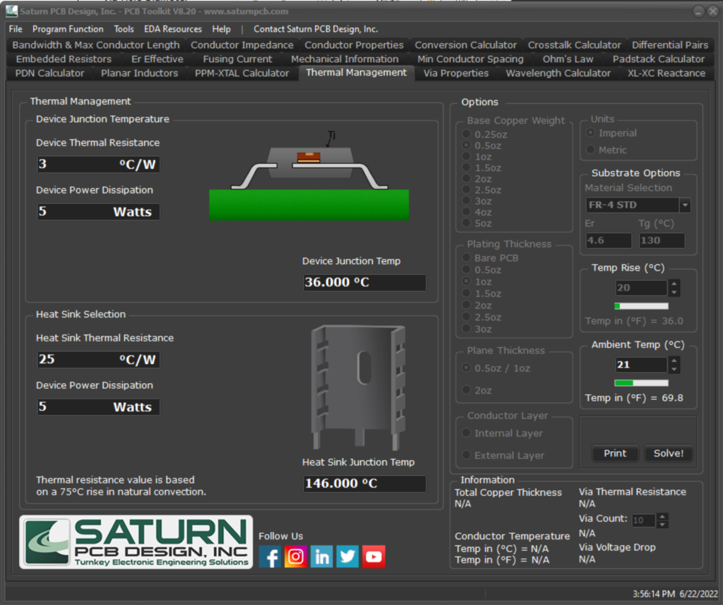
Device Junction Temperature:
Device Thermal Resistance:
This is the thermal resistance of the device in given in degrees C over Watts.
Device Power Dissipation:
This is the total power being dissipated in the device.
Device Junction Temperature:
This is the temperature at the device junction.
Heat Sink Junction Temperature:
Heat Sink Thermal Resistance:
This is the thermal resistance of the heat sink in given in degrees C over Watts.
Device Power Dissipation:
This is the total power being dissipated in the device.
Heat Sink Junction Temperature:
This is the temperature at the heat sink junction.
Via Properties
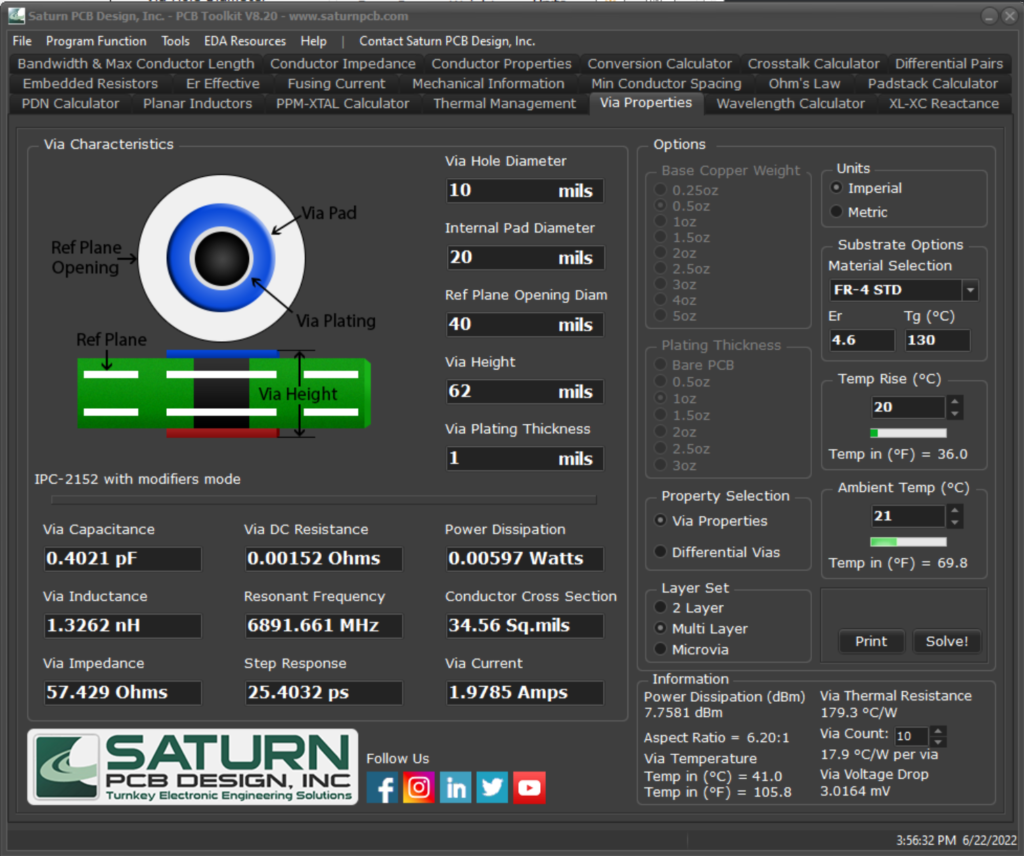
Via Properties:
Layer Set:
Choose between a 2 layer via, a multi-layer via and a microvia.
Via Hole Diameter:
This is the finished diameter the via hole.
Internal Pad Diameter:
This is the diameter of the inner layer pad for the via and is used for multi-layer impedance calculations.
Reference Plane Opening Diameter:
This is the diameter of the opening surrounding the internal pad. This value can’t be less than internal pad diameter.
Via Height:
This is the length of the via from its starting layer to its ending layer. The thinner a PCB is, the less heat it can dissipate thereby lowering the current needed in a via to raise its temperature.
Via Plating Thickness:
This is the thickness of copper plated into the via hole after drilling. Ask your vendor for the exact value to get a more accurate result as this value can vary.
Via Capacitance:
This is the approximated capacitance of the via with the given inputs. This value is only available for multi-layer vias as it uses the internal pad and reference plane opening for the calculation.
Via Inductance:
This is the approximated inductance of the via with the given inputs.
Via Impedance:
This is the approximated AC impedance of the via with the given inputs. This value is only available for multi-layer vias as it uses via capacitance for the calculation. via_zo = sqrt(via_l/ (via_c * 0.001))
Via DC Resistance:
This is the approximated DC resistance of the via with the given inputs.
Resonant Frequency:
This is the approximated resonant frequency of the via with the given inputs. This value is only available for multi-layer vias as it uses the via capacitance for the calculation.
Resonant Frequency:
This is the approximated resonant frequency of the via with the given inputs. This value is only available for multi-layer vias as it uses the
via capacitance for the calculation.
Step Response:
This is the step response of the via with the given inputs. It is the value of T10-90% step response and shows the impact on the rise time of a 50 Ohm transmission line.
Power Dissipation:
This is the approximated power dissipation of the via with the given inputs. It is found by the I2R method using the calculated values of via current and DC resistance.
Power Dissipation dBm:
This is the approximated power dissipation of the via with the given inputs converted to dBm.
Via Voltage Drop:
This is the DC voltage dropped across the via. V = I*R
Conductor Cross Section:
This is the approximated cross-sectional area of the via as compared to a flat conductor.
Via Current:
This is the approximated current that will cause the temperature of the via to rise to the level of the chosen temperature in the temperature rise edit box.
Via Voltage Drop:
This is the approximated voltage drop across the resistor based on its resistance and the current flowing through it.
Via Thermal Resistance:
This is the approximated thermal resistance of the via.
Via Count:
Enter the number of thermal vias desired and the calculator outputs the thermal resistance of each via.
Differential Vias:
NOTE:
This calculator assumes that all non-functional pads have been removed. Ex, a 16-layer board, with connections to one inner layer, would have 13 layers of non-functional via pads removed in order to not affect the via’s characteristics. See these articles for more information about this calculator:
Method of Modeling Differential Vias
Two-Resonator Method for Characterization of Dielectric Substrate Anisotropy
Drill Hole Diameter:
Please use the drill diameter for the via hole, not the finished hole diameter as in the Via Properties calculator.
Ref Plane Opening H / W:
Enter the opening size or anti-pad size for the via pads.
Full Plane Opening:
Use this checkbox if you prefer to have a full opening for the vias on the reference plane.
Via Spacing:
This is the center to center spacing of the two differential vias.
Anisotropy:
Enter the anisotropy of the PCB substrate. You may need to contact your material vendor for this as it is not always shown in material datasheets.
NOTE:
A material is anisotropic when there are different values for parallel (x-y) vs perpendicular(z) measured values for dielectric constant. See this paper for more information:
P.I. Dankov, V.N. Levcheva, B.N. Hadjistamov, “Two-Resonator Method for Characterization of Dielectric Substrate Anisotropy”, Bulgarian Journal of Physics, pp. 33-52, May 23,2008
Two-Resonator Method for Characterization of Dielectric Substrate Anisotropy
Baud Rate:
Enter the baud rate of the applied signal to determine maximum stub length.
Maximum Stub Length:
This is a calculated value for how long a via stub can be before encountering unwanted resonant frequency nulls.
Wavelength Calculator
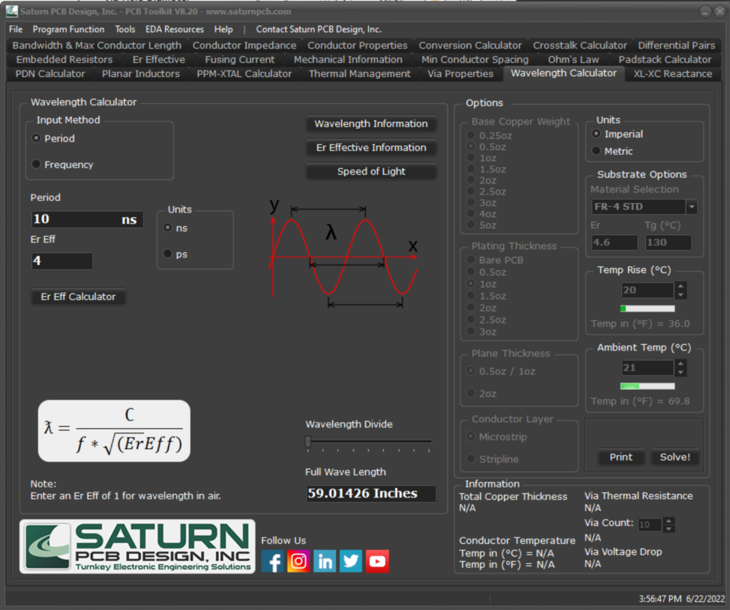
This program calculates the wavelength of a given frequency using Er effective and period / frequency. Note that Er effective is not always the substrate’s stated Er value.
Input Method:
Select between entering the signal’s period or frequency.
Er Eff:
Enter the effective dielectric constant of the material. If this is not known, the Er Eff Calculator can be used to help find this value.
Wavelength Divide:
Use the slider to show values of wavelength from Full to 1/20th constant.
XC-XL Reactance
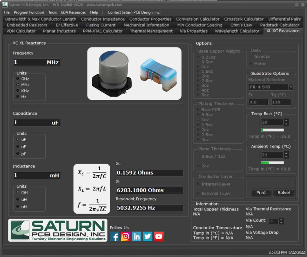
Solve for XC, XL and resonant frequency based of input frequency, capacitance and inductance
Frequency:
Enter the frequency of the signal applied to the capacitors / inductors.
Capacitance:
Enter the capacitance value in uF, nF or pF.
Inductance:
Enter the inductance value in mH, uH or nH.
Xc:
This is the capacitive reactance based on the given inputs.
Xl:
This is the inductive reactance based on the given inputs.
Resonant Frequency:
This is the resonant frequency between the inputted capacitance and inductance.
Program Options
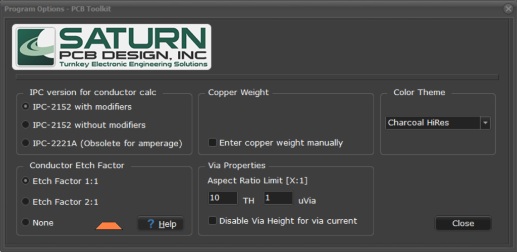
IPC Version:
The user can select the IPC version to use for current calculations.
We recommend using the IPC-2152 without modifiers for most applications.
The modifiers can be used when the user needs to minimize the conductor width as much as possible due to spacing constraints.
Copper Weight:
Enter Copper Weight Manually:
The user can select the option to enter base copper weight and plating thickness manually.
Conductor Etch Factor:
An ideal PCB conductor has a rectangular cross section but in reality, the real cross section is more trapezoidal due to the etching process. This changes the cross-sectional area of the conductor slightly which in turn affects current capacity. Conductor etch factor helps to model the conductor with a more real-world cross-sectional area. Typical etch factor is 1:1, meaning that the distance the conductor is etched on each side is equal to the conductor height. So, if we consider the bottom side of the conductor to equal H1 and the top side of the conductor to equal H2 then H2 = (H1-2T) where T is the conductor thickness. A 2:1 option is also available for etch factor where the ratio is half that of 1:1.
If you do not want this option, then select “None” as the etch factor.
Disable Via Height:
Per the IPC-2152 spec, the height of a via influences its heat dissipating capacity. This calculation can be disabled by checking the box if so desired.
Aspect ratio Limit:
You can set the aspect ratio for through hole vias and microvias in an X:1 format. If this rule is broken, the aspect ratio will turn red in the Via Properties tab information area.
Color Theme:
The user can select from one of five pre-installed color themes for the PCB Toolkit.
General Settings
Units:
Switches between Imperial (mils) and Metric (mm) units.
Base Copper Weight:
This is the thickness of the copper clad on the PCB substrate before plating.
Plating Thickness:
This is the thickness of copper added to the base copper clad by the manufacturer during the plating process.
Note: All external layers are plated with some amount of copper to obtain a PTH. Internal layers are not plated.
Material Selection:
Choose from a list of different PCB substrates to give predefined values of dielectric constants and glass temperatures or enter a custom dielectric constant or Tg in the edit boxes.
Temp Rise:
Enter the desired temp rise, or maximum temp rise, for your via or conductor. This is the amount, in Celsius, that a via or conductor will rise with the calculated amount of current flowing through it.
Ambient Temp:
Enter the ambient temperature of the device.
Dielectric Constant:
Dielectric constant of the base material. Some common substrates and their respective dielectric constants are provided in the dropdown list of materials.
Tg:
Glass transition temperature of the material. Some common substrates and their respective dielectric constants are provided in the dropdown list of materials.
Print:
Print, in graphical form, the data.
Solve:
Press enter in any input edit box.
Solve for the given inputs.